


Flip-flop (electronics)
In electronics, a flip-flop or latch is a circuit that has two stable states and can be used to store state information. The circuit can be made to change state by signals applied to one or more control inputs and will have one or two outputs. Flip-flops and latches are a fundamental building block of digital electronics systems used in computers, communications, and many other types of systems.
Flip-flops and latches are used as data storage elements. Such data storage can be used for storage of state, and such a circuit is described as sequential logic. When used in a finite-state machine, the output and next state depend not only on its current input, but also on its current state (and hence, previous inputs.) It can also be used for counting of pulses, and for synchronizing variably-timed input signals to some reference timing signal.
Flip-flops can be either simple (transparent or opaque) or clocked (synchronous or edge-triggered); the simple ones are commonly called latches.[1] The word latch is mainly used for storage elements, while clocked devices are described as flip-flops.[2]
Contents[hide]
|
[edit] History

The first electronic flip-flop was invented in 1918 by William Eccles and F. W. Jordan.[3][4] It was initially called the Eccles–Jordan trigger circuit and consisted of two active elements (vacuum tubes).[5] Such circuits and their transistorized versions were common in computers even after the introduction of integrated circuits, though flip-flops made from logic gates are also common now.[6][7]
Early flip-flops were known variously as trigger circuits or multivibrators. A multivibrator is a two-state circuit; they come in several varieties, based on whether each state is stable or not: an astable multivibrator is not stable in either state, so it acts as a relaxation oscillator; a monostable multivibrator makes a pulse while in the unstable state, then returns to the stable state, and is known as a one-shot; a bistable multivibrator has two stable states, and this is the one usually known as a flip-flop. However, this terminology has been somewhat variable, historically. For example:
- 1942 – multivibrator implies astable: "The multivibrator circuit (Fig. 7-6) is somewhat similar to the flip-flop circuit, but the coupling from the anode of one valve to the grid of the other is by a condenser only, so that the coupling is not maintained in the steady state."[8]
- 1942 – multivibrator as a particular flip-flop circuit: "Such circuits were known as 'trigger' or 'flip-flop' circuits and were of very great importance. The earliest and best known of these circuits was the multivibrator."[9]
- 1943 – flip-flop as one-shot pulse generator: "It should be noted that an essential difference between the two-valve flip-flop and the multivibrator is that the flip-flop has one of the valves biased to cutoff."[10]
- 1949 – monostable as flip-flop: "Monostable multivibrators have also been called 'flip-flops'."[11]
- 1949 – monostable as flip-flop: "... a flip-flop is a monostable multivibrator and the ordinary multivibrator is an astable multivibrator."[12]
According to P. L. Lindley, a JPL engineer, the flip-flop types discussed below (RS, D, T, JK) were first discussed in a 1954 UCLA course on computer design by Montgomery Phister, and then appeared in his book Logical Design of Digital Computers.[13][14] Lindley was at the time working at Hughes Aircraft under Dr. Eldred Nelson, who had coined the term JK for a flip-flop which changed states when both inputs were on. The other names were coined by Phister. They differ slightly from some of the definitions given below. Lindley explains that he heard the story of the JK flip-flop from Dr. Eldred Nelson, who is responsible for coining the term while working at Hughes Aircraft. Flip-flops in use at Hughes at the time were all of the type that came to be known as J-K. In designing a logical system, Dr. Nelson assigned letters to flip-flop inputs as follows: #1: A & B, #2: C & D, #3: E & F, #4: G & H, #5: J & K.
[edit] Implementation

Flip-flops can be either simple (transparent) or clocked; the transparent ones are commonly called latches.[1] The word latch is mainly used for storage elements, while clocked devices are described as flip-flops.[2]
Simple flip-flops can be built around a pair of cross-coupled inverting elements: vacuum tubes, bipolar transistors, field effect transistors, inverters, and inverting logic gates have all been used in practical circuits. Clocked devices are specially designed for synchronous systems; such devices ignore their inputs except at the transition of a dedicated clock signal (known as clocking, pulsing, or strobing). Clocking causes the flip-flop to either change or retain its output signal based upon the values of the input signals at the transition. Some flip-flops change output on the rising edge of the clock, others on the falling edge.
Since the elementary amplifying stages are inverting, two stages can be connected in succession (as a cascade) to form the needed non-inverting amplifier. In this configuration, each amplifier may be considered as an active inverting feedback network for the other inverting amplifier. Thus the two stages are connected in a non-inverting loop although the circuit diagram is usually drawn as a symmetric cross-coupled pair (both the drawings are initially introduced in the Eccles–Jordan patent).
[edit] Flip-flop types
Flip-flops can be divided into common types: the RS ("set-reset"), D ("data" or "delay"[15]), T ("toggle"), and JK types are the common ones. The behavior of a particular type can be described by what is termed the characteristic equation, which derives the "next" (i.e., after the next clock pulse) output, Qnext, in terms of the input signal(s) and/or the current output, Q.
[edit] Simple set-reset latches
[edit] SR NOR latch
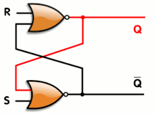
When using static gates as building blocks, the most fundamental latch is the simple SR latch, where S and R stand for set and reset. It can be constructed from a pair of cross-coupled NOR logic gates. The stored bit is present on the output marked Q.
While the S and R inputs are both low, feedback maintains the Q and Q outputs in a constant state, with Q the complement of Q. If S (Set) is pulsed high while R (Reset) is held low, then the Q output is forced high, and stays high when S returns to low; similarly, if R is pulsed high while S is held low, then the Q output is forced low, and stays low when R returns to low.
|

The symbol for an SR NOR latch
|
||||||||||||||||||||
The R = S = 1 combination is called a restricted combination or a forbidden state because, as both NOR gates then output zeros, it breaks the logical equation Q = not Q. The combination is also inappropriate in circuits where both inputs may go low simultaneously (i.e. a transition from restricted to keep). The output would lock at either 1 or 0 depending on the propagation time relations between the gates (a race condition). In certain implementations, it could also lead to longer ringings (damped oscillations) before the output settles, and thereby result in undetermined values (errors) in high-frequency digital circuits. Although this condition is usually avoided, it can be useful in some applications.
To overcome the restricted combination, one can add gates to the inputs that would convert (S,R) = (1,1) to one of the non-restricted combinations. That can be:
- Q = 1 (1,0) – referred to as an S-latch
- Q = 0 (0,1) – referred to as an R-latch
- Keep state (0,0) – referred to as an E-latch
Alternatively, the restricted combination can be made to toggle the output. The result is the JK latch.
Characteristic: Q+ = R'Q + R'S or Q+ = R'Q + S.[16]
[edit] SR NAND latch

This is an alternate model of the simple SR latch built with NAND (not AND) logic gates. Set and reset now become active low signals, denoted S and R respectively. Otherwise, operation is identical to that of the SR latch. Historically, SR-latches have been predominant despite the notational inconvenience of active-low inputs. This is because NAND gates are cheaper to produce than NOR gates in the diode-transistor logic (DTL), transistor-transistor logic (TTL) families, and complementary metal–oxide semiconductor (CMOS) logic families.
|

Symbol for an SR NAND latch
|
||||||||||||||||||||||
[edit] JK latch
The JK latch is much less used than the JK flip-flop. The JK latch follows the following state table:
| JK latch truth table | ||||
| J | K | Qnext | Comment | |
| 0 | 0 | Q | No change | |
| 0 | 1 | 0 | Reset | |
| 1 | 0 | 1 | Set | |
| 1 | 1 | Q | Toggle | |
Hence, the JK latch is an SR latch that is made to toggle its output when passed the restricted combination of 11. Unlike the JK Flip-Flop, in the JK latch, this is not a useful state because the speed of the toggling is not directed by a clock.[17]
[edit] Gated latches and conditional transparency
Latches are designed to be transparent. That is, input signal changes cause immediate changes in output; when several transparent latches follow each other, using the same clock signal, signals can propagate through all of them at once. Alternatively, additional logic can be added to a simple transparent latch to make it non-transparent or opaque when another input (an "enable" input) is not asserted. By following a transparent-high latch with a transparent-low (or opaque-high) latch, a master–slave flip-flop is implemented.
[edit] Gated SR latch

A synchronous SR latch (sometimes clocked SR flip-flop) can be made by adding a second level of NAND gates to the inverted SR latch (or a second level of AND gates to the direct SR latch). The extra gates further invert the inputs so the simple SR latch becomes a gated SR latch (and a simple SR latch would transform into a gated SR latch with inverted enable).
With E high (enable true), the signals can pass through the input gates to the encapsulated latch; all signal combinations except for (0,0) = hold then immediately reproduce on the (Q,Q) output, i.e. the latch is transparent.
With E low (enable false) the latch is closed (opaque) and remains in the state it was left the last time E was high.
The enable input is sometimes a clock signal, but more often a read or write strobe.
|

Symbol for a gated SR latch
|
[edit] Gated D latch

This latch exploits the fact that in the two active input combinations (01 and 10) of a gated SR latch R is the complement of S. The input NAND stage converts the two D input states (0 and 1) to these two input combinations for the next SR latch by inverting the data input signal. The low state of the enable signal produces the inactive "11" combination. Thus a gated D-latch may be considered as a one-input synchronous SR latch. This configuration prevents from applying the restricted combination to the inputs. It is also known as transparent latch, data latch, or simply gated latch. It has a data input and an enable signal (sometimes named clock, or control). The word transparent comes from the fact that, when the enable input is on, the signal propagates directly through the circuit, from the input D to the output Q.
Transparent latches are typically used as I/O ports or in asynchronous systems, or in synchronous two-phase systems (synchronous systems that use a two-phase clock), where two latches operating on different clock phases prevent data transparency as in a master–slave flip-flop.
Latches are available as integrated circuits, usually with multiple latches per chip. For example, 74HC75 is a quadruple transparent latch in the 7400 series.
|
Symbol for a gated D latch
|
The truth table shows that when the enable/clock input is 0, the D input has no effect on the output. When E/C is high, the output equals D.
[edit] Earle latch

The classic gated latch designs have some undesirable characteristics.[18] They require double-rail logic or an inverter. The input-to-output propagation may take up to three gate delays. The input-to-output propagation is not constant – some outputs take two gate delays while others take three.
Designers looked for alternatives.[19] A successful alternative is the Earle latch.[20] It requires only a single data input, and its output takes a constant two gate delays. In addition, the two gate levels of the Earle latch can be merged with the last two gate levels of the circuits driving the latch. Merging the latch function can implement the latch with no additional gate delays.[18]
The Earle latch is hazard free.[21] If the middle NAND gate is omitted, then one gets the polarity hold latch, which is commonly used because it demands less logic.[22][21] Intentionally skewing the clock signal can avoid the hazard.[22]
[edit] D flip-flop

The D flip-flop is the most common flip-flop in use today. It is better known as data or delay flip-flop (as its output Q looks like a delay of input D).
The Q output takes on the state of the D input at the moment of a positive edge at the clock pin (or negative edge if the clock input is active low).[23] It is called the D flip-flop for this reason, since the output takes the value of the D input or data input, and delays it by one clock cycle. The D flip-flop can be interpreted as a primitive memory cell, zero-order hold, or delay line. Whenever the clock pulses, the value of Qnext is D and Qprev otherwise.
Truth table:
-
-
Clock D Q Qprev Rising edge 0 0 X Rising edge 1 1 X Non-Rising X Qprev
-
('X' denotes a Don't care condition, meaning the signal is irrelevant)
Most D-type flip-flops in ICs have the capability to be forced to the set or reset state (which ignores the D and clock inputs), much like an SR flip-flop. Usually, the illegal S = R = 1 condition is resolved in D-type flip-flops. By setting S = R = 0, the flip-flop can be used as described above.
-
-
Inputs Outputs S R D > Q Q' 0 1 X X 0 1 1 0 X X 1 0 1 1 X X 1 1
-
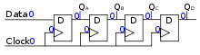
These flip-flops are very useful, as they form the basis for shift registers, which are an essential part of many electronic devices. The advantage of the D flip-flop over the D-type "transparent latch" is that the signal on the D input pin is captured the moment the flip-flop is clocked, and subsequent changes on the D input will be ignored until the next clock event. An exception is that some flip-flops have a "reset" signal input, which will reset Q (to zero), and may be either asynchronous or synchronous with the clock.
The above circuit shifts the contents of the register to the right, one bit position on each active transition of the clock. The input X is shifted into the leftmost bit position.
[edit] Classical positive-edge-triggered D flip-flop

This clever circuit[24] consists of two stages implemented by SR NAND latches. The input stage (the two latches on the left) processes the clock and data signals to ensure correct input signals for the output stage (the single latch on the right). If the clock is low, both the output signals of the input stage are high regardless of the data input; the output latch is unaffected and it stores the previous state. When the clock signal changes from low to high, only one of the output voltages (depending on the data signal) goes low and sets/resets the output latch: if D = 0, the lower output becomes low; if D = 1, the upper output becomes low. If the clock signal continues staying high, the outputs keep their states regardless of the data input and force the output latch to stay in the corresponding state as the input logical zero remains active while the clock is high. Hence the role of the output latch is to store the data only while the clock is low.
The circuit is closely related to the gated D latch as both the circuits convert the two D input states (0 and 1) to two input combinations (01 and 10) for the output SR latch by inverting the data input signal (both the circuits split the single D signal in two complementary S and R signals). The difference is that in the gated D latch simple NAND logical gates are used while in the positive-edge-triggered D flip-flop SR NAND latches are used for this purpose. The role of these latches is to "lock" the active output producing low voltage (a logical zero); thus the positive-edge-triggered D flip-flop can be thought as of a gated D latch with latched input gates.
[edit] Master–slave pulse-triggered D flip-flop
A master–slave D flip-flop is created by connecting two gated D latches in series, and inverting the enable input to one of them. It is called master–slave because the second latch in the series only changes in response to a change in the first (master) latch.
The term pulse-triggered means that data is entered on the rising edge of the clock pulse, but the output does not reflect the change until the falling edge of the clock pulse.[dubious ]


For a positive-edge triggered master–slave D flip-flop, when the clock signal is low (logical 0) the "enable" seen by the first or "master" D latch (the inverted clock signal) is high (logical 1). This allows the "master" latch to store the input value when the clock signal transitions from low to high. As the clock signal goes high (0 to 1) the inverted "enable" of the first latch goes low (1 to 0) and the value seen at the input to the master latch is "locked". Nearly simultaneously, the twice inverted "enable" of the second or "slave" D latch transitions from low to high (0 to 1) with the clock signal. This allows the signal captured at the rising edge of the clock by the now "locked" master latch to pass through the "slave" latch. When the clock signal returns to low (1 to 0), the output of the "slave" latch is "locked", and the value seen at the last rising edge of the clock is held while the "master" latch begins to accept new values in preparation for the next rising clock edge.
By removing the leftmost inverter in the circuit at side, a D-type flip flop that strobes on the falling edge of a clock signal can be obtained. This has a truth table like this:
-
-
D Q > Qnext 0 X Falling 0 1 X Falling 1
-

[edit] Edge-triggered dynamic D flip-flop
A more efficient way to make a D flip-flop is not so easy to understand, but it works the same way. While the master–slave D flip-flop is also triggered on the edge of a clock, its components are each triggered by clock levels. The "edge-triggered D flip-flop" does not have the master–slave properties.
Edge-triggered D flip-flops are often implemented in integrated high-speed operations using dynamic logic. This means that the digital output is stored on parasitic device capacitance while the device is not transitioning. This design of dynamic flip flops also enable simple resetting since the reset operation can be performed by simply discharging one or more internal nodes. A common dynamic flip-flop variety is the True Single Phase Clock (TSPC) which performs the flip flop operation with little power and at high speeds. However these types of dynamic flip-flops will not work at static or low clocked speeds, since given enough time the parasitic capacitance will discharge through leakage paths and will cause the logic levels to enter invalid states.
[edit] T flip-flop

If the T input is high, the T flip-flop changes state ("toggles") whenever the clock input is strobed. If the T input is low, the flip-flop holds the previous value. This behavior is described by the characteristic equation:
 (expanding the XOR operator)
and can be described in a truth table:
| T flip-flop operation[25] | ||||||||
|---|---|---|---|---|---|---|---|---|
| Characteristic table | Excitation table | |||||||
| T | Q | Qnext | Comment | Q | Qnext | T | Comment | |
| 0 | 0 | 0 | hold state (no clk) | 0 | 0 | 0 | No change | |
| 0 | 1 | 1 | hold state (no clk) | 1 | 1 | 0 | No | |
نظرات شما عزیزان:

